


At a time when the benefits of chip process technology have peaked, 2.5D packaging, with its three-dimensional 'bridging' integration approach, has become the core driving force for high-performance computing in the 'post-Moore' era. However, this dense integration also brings fundamental thermal challenges—heat accumulates intensely in tiny spaces, which has evolved from a design consideration into a critical bottleneck that limits both chip performance and reliability.
The Threefold Thermal Challenges of 2.5D Packaging
The heterogeneous integration architecture of 2.5D packaging results in unprecedented complexity in heat transfer paths and thermal stress distribution, presenting three main core challenges: a dramatic increase in heat flux density; extrusion of interface materials due to height differences in stacked layers; and poor interface contact caused by chip warpage.
Thermal Interface Materials as the Key Nexus Determining Heat Dissipation Efficiency
In the entire heat dissipation chain, thermal interface materials act as the 'thermal bridge' connecting the heat source to the cooling structure. Their performance directly determines over 60% of interface thermal resistance, making them the core element in solving heat dissipation challenges.

At the core interface between the chip and the heat spreader, the materials face significant challenges: they not only require extremely high thermal conductivity to cope with rapid temperature rises but must also possess excellent compliance to compensate for chip warping and height differences among multiple chiplets. The 'pump-out' effect of traditional high-performance thermal grease and the complex soldering process of indium sheets both struggle to simultaneously meet reliability and large-size compatibility requirements. At the interface between the heat spreader and the external cooler, technical demands shift toward system integration friendliness, emphasizing the material's compressive resilience, ease of assembly, and long-term stability. In summary, from addressing internal microscopic deformations to meeting external macroscopic assembly needs, comprehensive innovation in thermal interface materials has become key to advancing the heat dissipation capability of advanced packaging.
HFC Graphene Thermal Pad: Innovative Breakthrough for 2.5D Package TIM1 Interface
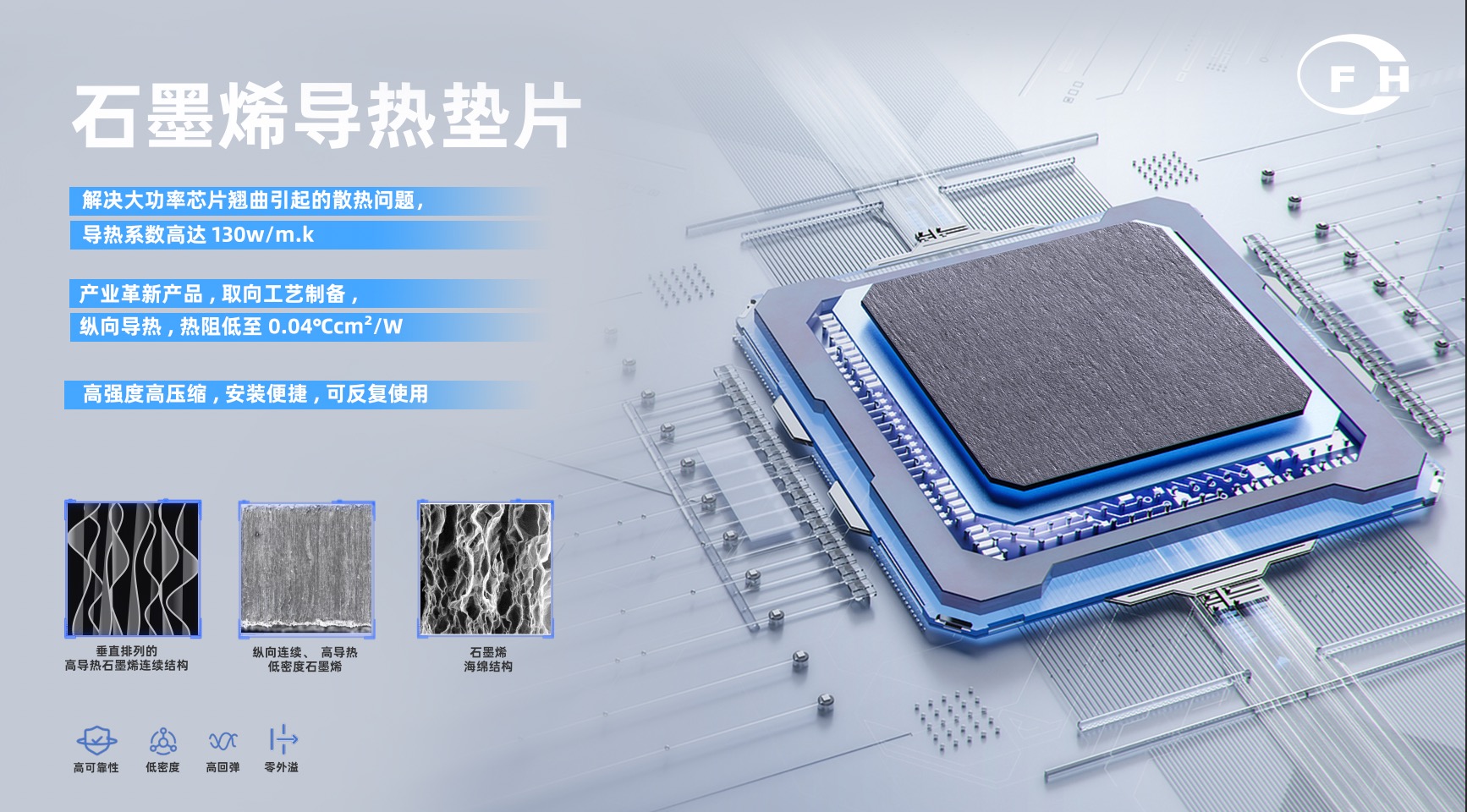
Material Characteristics:
Three Core Advantages Reshaping Thermal DissipationAddressing the core challenges of 2.5D package thermal interface materials, HFC has developed a graphene thermal pad based on vertical orientation technology, creating an innovative solution characterized by 'high thermal conductivity, warp resistance, and long-term stability,' making it an ideal choice for overcoming thermal dissipation bottlenecks.High Thermal Conductivity: Through a special fabrication process, HFC graphene thermal pads achieve a thermal conductivity of 130 W/mK, with thermal resistance as low as 0.04℃·cm²/W;High Resilience: Excellent flexibility and rebound, allowing up to 70% compression;Long-Term Reliability: Graphene itself has strong chemical inertness, and combined with process design, it prevents issues common in traditional materials such as pump-out, drying, and creep.
Precision Applications:
Directly Tackling the Core Challenges of 2.5D PackagingBy applying Hongfucheng's graphene thermal pads in packaging, directly covering the back of core chips such as GPU and HBM, three key benefits can be achieved:Cross-height Thermal Conduction: Highly compressible and self-adapting to different heights, eliminating hard-to-cover thermal dead spots;Warping Suppression: Flexible structure absorbs thermo-mechanical stress, preventing thermal resistance spikes caused by interface separation, ensuring long-term thermal stability;Simplified Process and Cost: No need for gold plating, reflow soldering, or other steps, significantly reducing production investment and time costs compared to materials like indium sheets.
In the era where computing power reigns, HFC leverages material innovation to solve thermal challenges, unlocking the potential of 2.5D packaging and providing sustained power for AI, HPC, and data centers.


 返回列表
返回列表 

